Schematic
Overview
The core circuit external cluster circuit of TXW8Ix series chips includes 1 passive crystal, 1 FLASH (some models have built-in FLASH), and a small amount of capacitors.
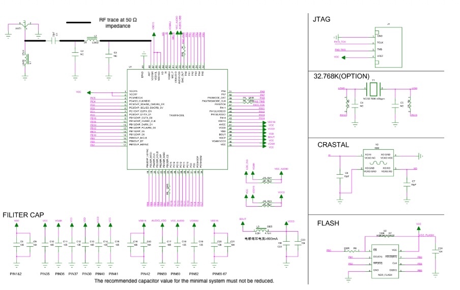 TXW818-C08L Minimum System
Power Supply
Power supply pins
| Name | Output/Input | DC Characteristics(V) Min/Typ/Max | Description |
|---|---|---|---|
| VCCPA VCCRF | IN | 3.0/3.3/3.6 | RF power supply 3.3V input requires placing 106 and 104 capacitors close to the pins |
| VCC | IN | 3.0/3.3/3.6 | External power input, placing a 105 capacitor near the pin |
| VCC1/VCAM | IN/OUT | 1.8/2.8/3.3 | Inside the chip, VCAM and VCCI are connected together. VCAM has an internal LDO output. VOCI is a IO PB[6:15] and PC[0:2] IO power configuration pin. When VCAM outputs, it can supply power to external cameras or other peripherals, roughly arranged near the chip with a 105 capacitor |
| VCCP | IN | 3.0/3.3/3.6 | Placing a 105 capacitor near the chip pins at the internal DCDC power input. |
| BOUT | OUT | The SW pin of the internal DCDC is connected to a 4.7µH inductor along with the SW and controller pins, and the other end of the inductor needs to be connected to a 10µF and 100nF capacitor; this low-power solution is commonly used. The internal DCDC generally provides power to VCCD and VDDI5, while other schemes can bypass these components. | |
| VDD | IN/OUT | 1.05/1.1/1.18 | The chip core power is supplied by the internal LDO output to VDD by default. For low-power applications, an external DCDC can be connected. Place a 105 capacitor near the chip pins (the capacitance value must not be changed arbitrarily, otherwise it will cause abnormal chip operation). |
| VCCD | IN | 1.5/3.3/3.6 | A 105 capacitor should be placed at the LDO input of the internal VDD power supply, close to the chip pin. |
| VCCA | IN | 3.0/3.3/3.6 | Analog power input, placing a 105 capacitor close to the pin. |
| VDD18 | OUT | 1.0/1.8/2.55 | Internal LDO output, powers the internal PSRAM of the chip or provides power to the external CAMERA IO, placing 106+104 capacitors close to the pin. |
| AUDIOVDD | OUT | 2.5/2.7/2.8 | Internal LDO output, can provide bias voltage to the MIC, placing a 105 capacitor close to the pin. |
| V33AUDIO | IN | 3.0/3.3/3.6 | Audio power supply 3.3V input, placing a 105 capacitor close to the pin. |
| VCMAU | OUT | - /1.0/ - | Audio Common-Mode Power output, placing a 105 capacitor close to the pin. |
| VDD15O VDD15L VDD15R | OUT IN IN | - /1.8/ - | The RF power supply VDD150 outputs 1.5V to supply VDD15L and VDD15R, and the PCB design connects them together, placing 106+104 capacitors close to the pin. |
Notice:
- The power supply pin capacitors recommended in the above table should not be arbitrarily removed, otherwise it may affect system stability or RF performance.
- VDD is the core voltage. When using an external DC-DC supply, it is important to ensure that the power ripple noise does not exceed 30mV.
- VDD needs to take into account the voltage drop along the PCB traces, usually about 20mV higher than the required voltage.
- If the product involves hot-plug, please confirm before mass production that live plugging will not cause power overvoltage. During hardware design, proper surge protection circuits should be reserved; otherwise, it can easily cause permanent physical damage to the chip.
Boot Mode
Flash and PSRAM
External SPI Flash
| GPIO | SPI FLASH |
|---|---|
| PB0 | CS |
| PB1 | IO1 |
| PB2 | IO2 |
| PB3 | IO3 |
| PB4 | CLK |
| PB5 | IO0 |
Clock Source
External Crystal Clock Source
- External 40MHz crystal
RTC Clock Source(Optional)
- Internal 32K RTC
- External 32.768 kHz crystal