PCB Layout Guide
A good PCB design needs to consider the signal source, the switching bounce and the impedance matching on the transmission line, so that the wave can be low and the signal can be reflected in the transmission process. The impedance control of the single signal line depends on the relative position of the reference plane and the width of the signal starting line. The impedance control of the differential pair requires the width and distance of the differential pair depending on the layered structure of the PCB. In the specific product design, it is necessary to consider the cost and the minimum protrusion distance factor of the PCB, and choose the appropriate PCB stacking to achieve all the impedances on the board.
It is recommended to use a two-layer PCB design.
Power Supply
3.3V Input
The pins that require a 3.3V input are VCCPA, VCCRF.VCC, VCCP, VCCD (non-low-power applications need to connect to 3.3V), AVCC, and V33AUDIO.
When the power supply is provided by an external DCDC to 3.3V, the ripple of the 3.3V power must not exceed 50mV. The PCB traces should primarily ensure a current-carrying capacity of over 1A, and the minimum point should have at least 500mA overcurrent capability. All decoupling capacitors for power pins should be placed as close as possible to the power pins. If the chip's 3.3V shares a single power source, the PCB traces need to follow a star topology to reduce mutual interference among power lines. The power must pass through decoupling capacitors before being connected to the chip's power pins, and each decoupling capacitor's ground should have 1-2 nearby vias to ensure a short return path to the chip's EPAD.
3.3V Power Supply Layout
Notice: It is necessary to place the power or IO vias under the chip's EPAD, and you must ask the PCB manufacturer to ensure the via solder mask process is done correctly; otherwise, it can easily cause chip short circuits or other abnormal issues.
VDD Input
Under most use cases, VDD does not require an external DCDC. If it is a low-power solution and the scheme has special power consumption requirements, an external DCDC can be connected. The output voltage of the DCDC should be adjusted according to the actual requirements of the scheme or confirmed with the FAE. The ripple of the DCDC power supply should not exceed 30mV. During PCB layout, it is necessary to ensure that the PCB width at the narrowest part can handle at least 500mA of current. The external DCDC input should first pass through a decoupling capacitor before being connected to the chip's VDD pin, and the decoupling capacitor should be connected to the chip EPAD ground through 1-2 nearby ground vias.
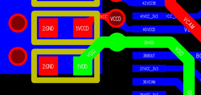 VDD Power Supply Layout
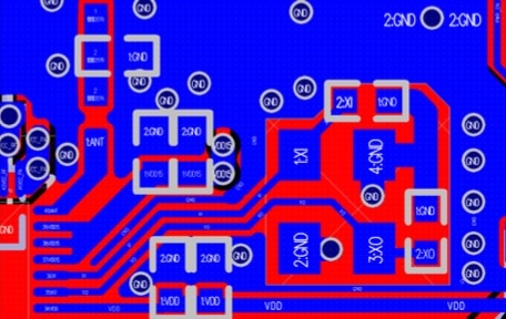
RF VDD15 Power
VDD15O is the internal LDO of the chip that supplies power to the RF VDD15R and VDD15L. During hardware design, these three pins are adjacent, so on the PCB the traces need to be routed out of the pad first and then connected together externally (if the three pads are connected directly, SMT soldering may easily cause poor solder joint issues). The decoupling capacitors are a combination of 106 and 104. During PCB design, these two capacitors should be placed on the same layer as the main control chip, and the capacitors should be placed as close as possible to the chip's power pins. The grounding of this set of capacitors should not have a direct return path on the same layer as the crystal ground, otherwise it may affect RF performance.
RF VDD15 Power Layout
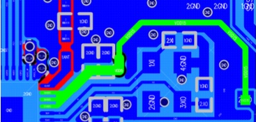
BOUT Output
Keep the connections of BOUT, the inductor, and VCCD as short as possible (BOUT is the SW output of the internal DCDC, so the wiring should be as short as possible). Place the filter capacitor close to the chip pin, and route the capacitor's GND through vias to quickly return to the ground under the chip EPAD. The GND connection must not be interrupted by other traces to ensure that the return path for the inductor, capacitor, and chip is as short as possible. The bottom of the inductor should have a complete ground plane to avoid board-level EMI that could affect the sensitivity of the RF RX interface.
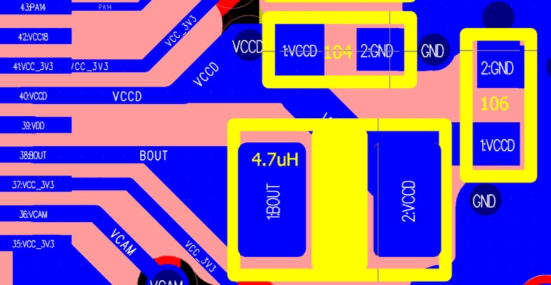
BOUT Output Layout
Cystal
Crystal Layout
RF
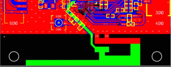
Crystal Antena Layout
Audio
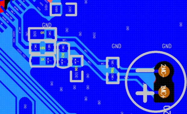
Audio Input Layout
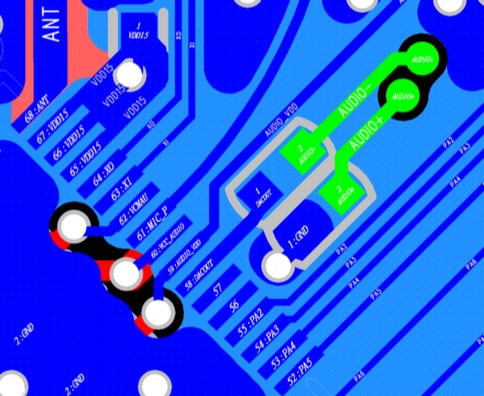
Audio Output Layout
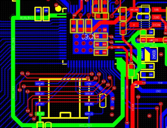
SPI Flash
The layout for SPI Flash signal designrequirements:
- The SPI FLASH shares a 3.3V power supply with the chip VCC. Place a 105 capacitor near the FLASH power pin and connect it in parallel to ground.
- The ground of the SPI FLASH should be connected to the ground at the bottom of the chip's EPAD as soon as possible. Do not split the ground between the two chips, otherwise it may affect RF performance.
- The CS and DATA routing of FLASH is based on CLK, with error control kept within 100 mils.
- Signal routing should avoid crossing power split areas and maintain the integrity of the signal reference plane.
- Route the CLK lines with ground on both sides. Place an RC low-pass filter network near the chip pin of the CLK signal to reduce EMI interference. For RF or certified designs, avoid revisions.
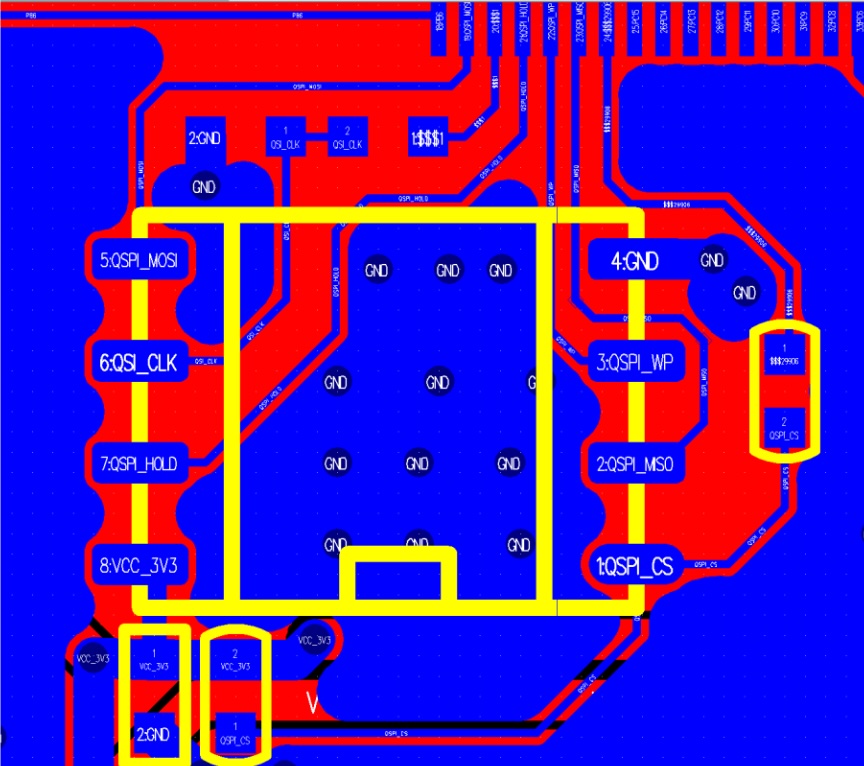
SPI Flash Layout